This is an old revision of the document!
Table of Contents
Peripheral Management in RPi
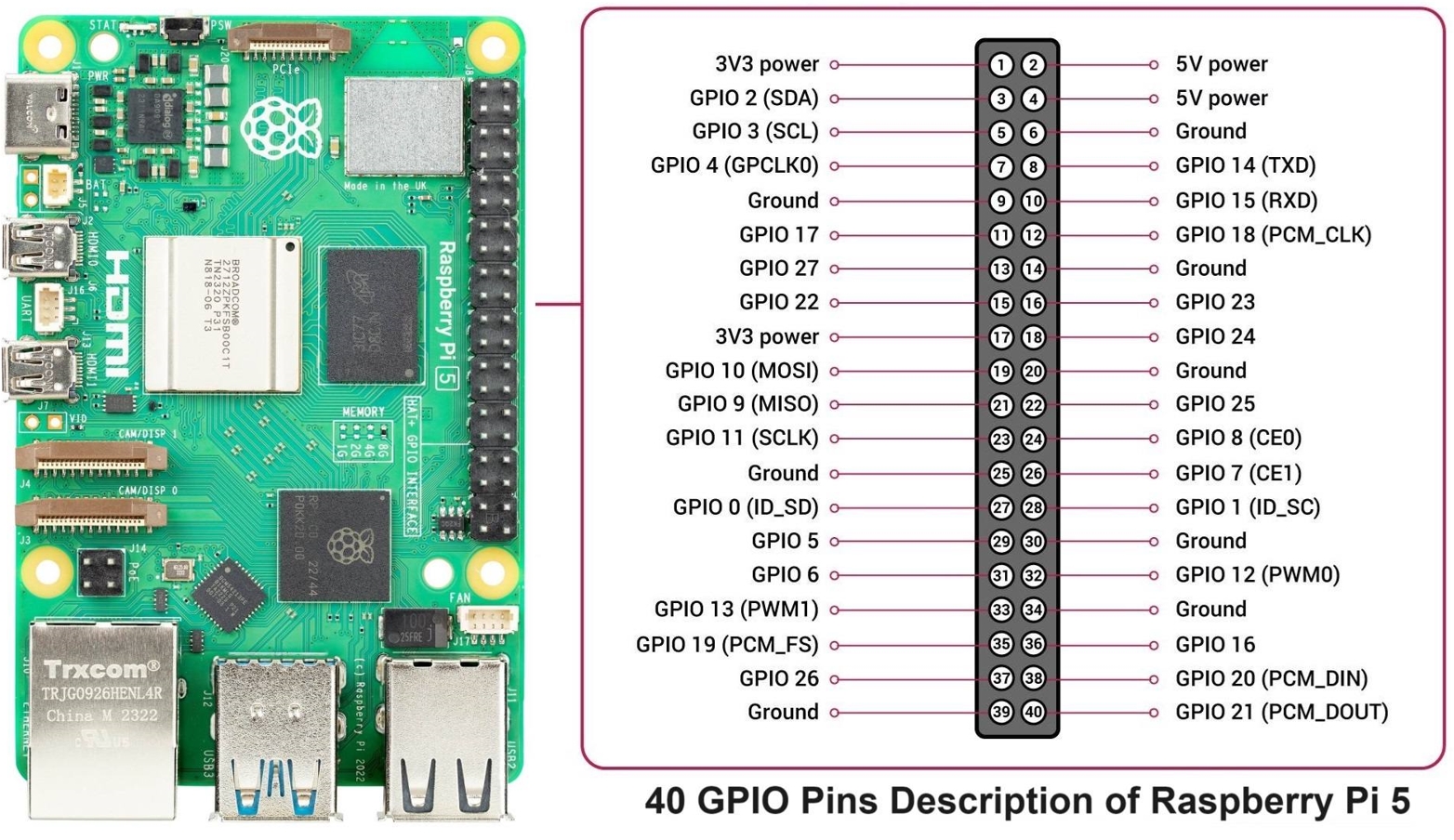
The Raspberry Pi has ported out some General-Purpose Input/Output (GPIO) lines. Several lines share functionality across the board's peripherals. To access peripherals like GPIO, they must be enabled in the Raspberry Pi 5 OS. Many things can be done with the Raspberry Pi's available GPIOs. In the picture below, the GPIOs and their alternative functions (in scope) are shown.
For example, to enable UART communication on GPIO 14 and 15, the “./boot/config.txt” file must be edited by adding these two lines:
dtoverlay=uart0-pi5dtparam=uart0=on
There are libraries designed to work with GPIO and/or communication interfaces such as UART, SPI, and I2C. For example, to work with GPIO, a special library in C or Python can be used, or GPIO can be accessed via memory mapping of IO registers. Note that GPIO parameters must be set before using them as outputs or inputs, like setting pull-up or pull-down resistors, setting direction, etc. On Linux, using libraries such as libgpiod or wiringPi/pigpio can save a lot of time. But these libraries are primarily available in C or even higher-level programming languages. The hardest part is to find proper hardware addresses. The Raspberry Pi5 installer RP1 peripheral controller documentation contains two addresses: System-Address, which is 40-bit long, and Proc-Address, which is 32-bit long. Taking the example of peripherals on the APB0 internal bus, the address in Proc-Address is 0x40000000, but in System-Address it is 0xC040000000. The difference is coloured out. Similar differences appear across all other peripheral buses, and these differences may occur in the code depending on the OS version, installed libraries, and drivers.
General Purpose Inputs and Outputs (GPIO)
Usable GPIO pins on the Raspberry Pi 5 are in IO_BANK0, and this provides information on the addresses available for GPIO programming. Other banks, IO_BANK1 and IO_BANK2, are reserved for internal use inside the board. The base address for IO_BANK0 is 0x400D0000, and the remaining addresses for GPIO programming are documented in the section “3.1.4.Registers” at the RP1 datasheet.
In the previous section, the basic GPIO pin toggling was implemented. GPIOs can be used for many purposes, such as replacing hardware components that are not available on the current board. The technique is called bit-banging. A Raspberry Pi has only one I2C interface, and let's assume that two or more sensors must be connected to the board and share the same I2C device address. This means that only one sensor per I2C channel can be connected, and as the Raspberry Pi has only one interface, only one sensor can be used. With the bit-bang technique, it is possible to create many communication interfaces if at least two GPIO pins are available. Note that the bit-banging technique uses processor power, so there are also limits for the number of interfaces. That’s because I2C must maintain a 100kHz clock rate for successful communication, and bit-banging techniques require significant processor power. Under heavy CPU load, the emulated I2C interfaces may run slower than necessary.
The following code example will be executed in the User space and may require root permissions to access the “/dev/gpiomem” device.
.global _start
.section .text

@ Constants
.equ GPIO_BASE,  0x400D0000
.equ GPFSEL0,    0x00
.equ GPSET0,     0x1C
.equ GPCLR0,     0x28
.equ GPLEV0,     0x34

.equ SDA_BIT,    (1 << 2)
.equ SCL_BIT,    (1 << 3)

_start:
    @ Open /dev/gpiomem (fd=3)
    MOV X8, #56              @ syscall openat
    MOV X0, #-100            @ AT_FDCWD
    LDR X1, =path
    MOV X2, #2               @ O_RDWR
    MOV X3, #0
    SVC #0                   @ open -> fd in X0
    MOV X19, X0              @ save fd

    @ mmap GPIO
    MOV X8, #222             @ syscall mmap
    MOV X0, #0               @ addr
    MOV X1, #4096            @ length
    MOV X2, #3               @ PROT_READ|PROT_WRITE
    MOV X3, #1               @ MAP_SHARED
    MOV X4, X19              @ fd
    MOV X5, #0               @ offset
    SVC #0
    MOV X20, X0              @ base addr

    @ configure pins 2,3 as outputs
    LDR W1, [X20, #GPFSEL0]
    BIC W1, W1, #(0b111 << 6)    @ clear bits for GPIO2
    ORR W1, W1, #(0b001 << 6)    @ set output
    BIC W1, W1, #(0b111 << 9)    @ clear bits for GPIO3
    ORR W1, W1, #(0b001 << 9)
    STR W1, [X20, #GPFSEL0]

    @ Send start condition: SDA low while SCL high
    BL scl_high
    BL delay
    BL sda_low
    BL delay

    @ Send byte 0xA5 (1010 0101)
    MOV W0, #0xA5
    MOV W1, #8
send_bit:
    BL scl_low
    TST W0, #0x80
    BEQ send_zero
    BL sda_high
    B after_bit
send_zero:
    BL sda_low
after_bit:
    BL delay
    BL scl_high
    BL delay
    BL scl_low
    LSL W0, W0, #1
    SUBS W1, W1, #1
    B.NE send_bit

    @ Stop: SDA high while SCL high
    BL sda_low
    BL scl_high
    BL delay
    BL sda_high

    @ Exit
    MOV X8, #93
    MOV X0, #0
    SVC #0

@ ---- Subroutines ----
sda_high:
    MOV W2, #SDA_BIT
    STR W2, [X20, #GPSET0]
    RET
sda_low:
    MOV W2, #SDA_BIT
    STR W2, [X20, #GPCLR0]
    RET
scl_high:
    MOV W2, #SCL_BIT
    STR W2, [X20, #GPSET0]
    RET
scl_low:
    MOV W2, #SCL_BIT
    STR W2, [X20, #GPCLR0]
    RET
delay:
    MOV W3, #100
delay_loop:
    SUBS W3, W3, #1
    B.NE delay_loop
    RET

.section .rodata
path: .asciz "/dev/gpiomem"
Overall, working with any peripheral requires studying its documentation to identify its base addresses and the offset addresses needed to control it.


